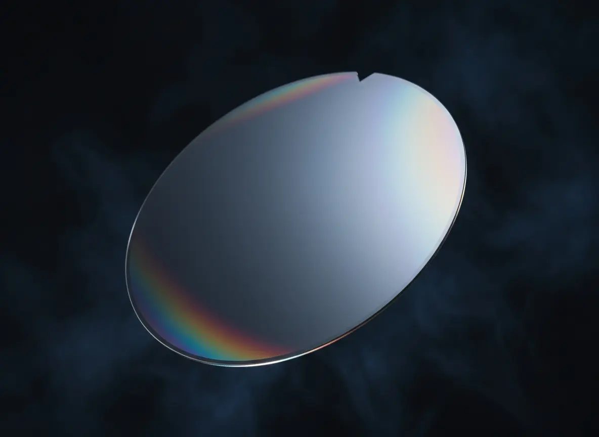
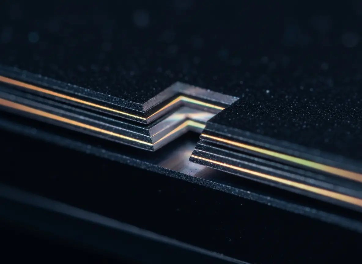
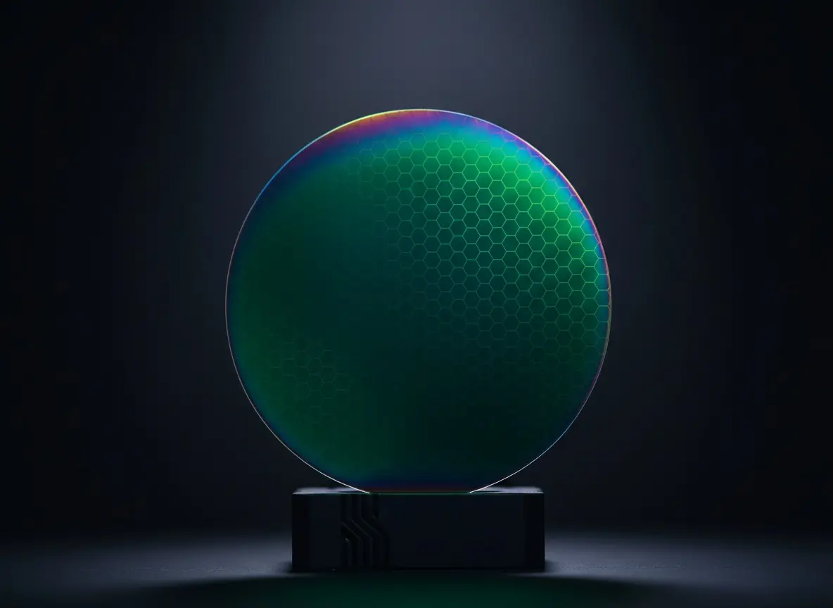
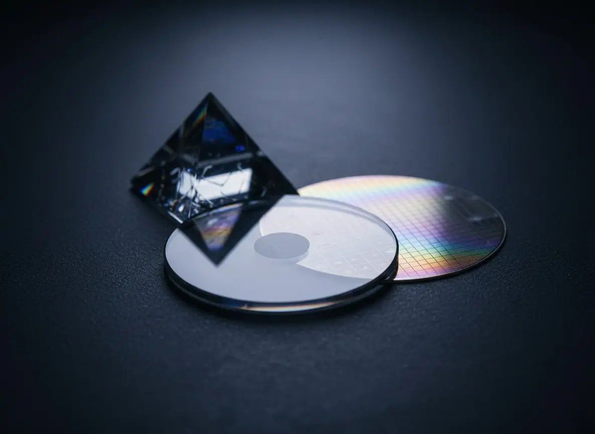
We combine decades of experience, strong global partnerships, and in-house slicing and polishing to deliver wafers that meet even the most demanding specifications.
Ready-to-Ship
Standard wafers and hard-to-find specifications, in stock and ready to ship.
Hundreds of standard wafer specifications, alongside uncommon orientations and ultra-flat wafers, ship same day from New Jersey.
25mm–300mm silicon, InP, GaAs, Ge, quartz, sapphire, and more
TTV <10 µm standard, <1 µm regularly, <0.5 µm upon special request
With a large inventory of silicon ingots, in-house slicing and polishing, and advanced metrology including our ADE 9500, capable of measuring thousands of points across each wafer, we can produce wafers to specifications that are difficult to source off the shelf. Our global partners also provide custom FZ and CZ ingots, silicon wafers, and other semiconductor materials.
Thickness tolerance: ±25 µm standard, ±2 µm upon request
Non-standard diameters & orientations
TTV <0.5 µm, Bow <5 µm, Warp <10 µm upon special request
Special pricing is available for full ingots as specified, F.O.B. Ridgefield Park, NJ with a typical lead time of 3–5 weeks ARO (subject to confirmation at the time of order). Pricing is subject to adjustment based on applicable tariff changes, and additional inventory may be available upon request.
Why EL-CAT
Engineered around your needs.
We align our materials, processes, and support around your exact requirements so you can move forward with confidence, whether you need standard wafers or highly specialized solutions.
ReachREASON · 01 / 05
Global availability: material in fabs across North America, Europe, and Asia.
SpeedREASON · 02 / 05
Speed without compromise: your spec leaves the shelf the same week.
PrecisionREASON · 03 / 05
Built for precision: diameter, doping, resistivity, orientation, verified before ship.
Real human support: engineers on the phone, spec questions answered same day.
01 · Purifying the Silicon
Purifying the Silicon
We begin with raw silicon that is refined into ultra-high-purity material. This removes nearly all impurities and creates the foundation for reliable electrical performance.
Removes residual metals, oxides, and carbon down to ppb-level traces
Sets the baseline for downstream consistency
Verified before every batch enters the growth line
02 · Growing a Single Crystal
Growing a Single Crystal
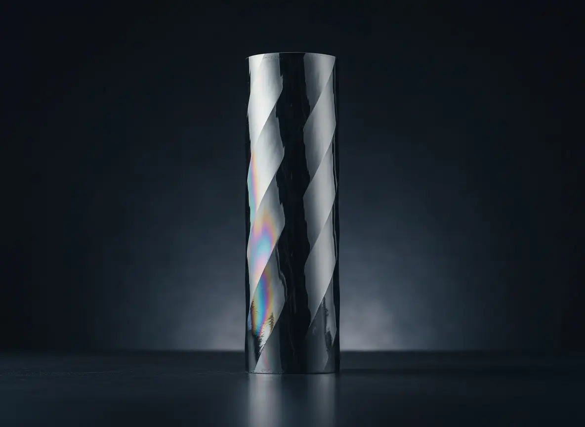
The purified silicon is melted and carefully formed into a single continuous crystal (an ingot). This step defines the structural integrity of every wafer that follows.
Float-zone and Czochralski lines, both run in-house
Doping profile dialled in during growth, not after
Diameters from 2" through 12" — seeded and pulled on site
03 · Slicing the Wafer
Slicing the Wafer
The silicon ingot is precisely cut into ultra-thin wafers using diamond wire saws. Each slice must meet strict requirements for uniformity and thickness.
Diamond wire sawing for clean, low-kerf cuts
Thickness, TTV, and bow controlled per wafer
Reject criteria measured in micrometres, not millimetres
04 · Polishing & Finishing
Polishing & Finishing
Each wafer is polished to an ultra-flat, mirror-like surface and then cleaned and inspected to ensure it meets exacting quality standards.
Mechanical + chemical polish — epi-ready surfaces
Every wafer cleaned, dried, and inspected before pack-out
Spec sheet + signed CoC ship inside every crate
05 · Custom Silicon Wafers by El Cat
Custom Silicon Wafers by El Cat
Not every application is the same—which is why El Cat specializes in custom wafer solutions tailored to specific performance needs. We customize:
Diameter and thickness
Crystal orientation
Resistivity and doping levels
Surface finish and polish specifications
Application-driven requirements
From the fab floor
What engineers say.
★★★★
We needed a very specific substrate configuration for a prototype project and couldn’t find it through our usual suppliers. EL-CAT not only sourced it quickly, but helped us refine the specs to ensure compatibility. Turnaround was faster than expected and the quality was exactly what we needed.
AR
Dr. Anika ReyesMaterials Lead, Photonics
★★★★★
EL-CAT has become one of our most reliable suppliers for both standard wafers and specialty materials. The ability to move between off-the-shelf inventory and custom orders without switching vendors has streamlined our entire procurement process.
MT
Marcus TanProcurement, Power Device Fab
★★★★★
What stands out most is their responsiveness and technical understanding. We’ve worked with them on multiple custom wafer requests, and they’ve consistently delivered materials that meet very tight specifications without delays or back-and-forth confusion.
LS
Prof. Liana SchultzSemiconductor Physics, ETH
Ready when you are
Get what you need, when you need it.
Two ways to move forward — pick the one that fits where you are.